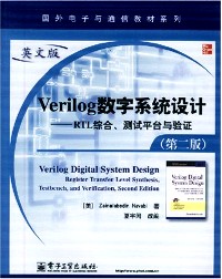
Verilog digital system design:register transfer level synthesis, testbench, and verification
副标题:无
作 者:(美)Zainalabedin Navabi著;夏宇闻改编
分类号:
ISBN:9787121052415
微信扫一扫,移动浏览光盘
简介
本书主要讲述基于IEEE Std 1364—2001版本的Verilog硬件描述语言
,着重讲述了使用Verilog进行数字系统的设计、验证及综合。根据数字集
成电路设计的工程需求,本书重点关注了testbench的设计编写、验证和测
试技术,深入讲述了基于VerilogHDL的开关级、门级、RTL级、行为级和系
统级建模技术,从而使读者能尽快掌握硬件电路和系统的高效’Vetilog编
程技术。书中把RTL描述、电路综合和testbench验证测试技术紧密结合,
给出了多个从设计描述到验证的RTL数字电路模块和系统的设计实例。改编
者在对标题、重点句子和段落进行注解时,在翻译的基础上针对较难理解
的内容做了详细说明。
本书的设计与讲解由浅入深,既适合高年级本科生作为双语教学教材
,也适合作为研究生第一年的双语课程教材。作为本科生和研究生数字系
统设计和计算机组织结构的补充,本书也很有价值。
目录
Chapter 1 Digital System Design Automation with Verilog
1.1 Digital Design Flow
1.1.1 Design entry
1.1.2 Testbench in Verilog
1.t.3 Design validation..:
1.1.4 Compilation and synthesis
1.1.5 Postsynthesis simulation
1.1.6 Timing analysis
1.1.7 Hardware generation
1.2 Verilog HDL
1.2.1 Verilog evolution
1.2.2 Verilog attributes
1.2.3 The Verilog language
1.3 Summary
Problems
Suggested Reading
Chapter 2 Register Transfer Level Design with Verilog
2.1 RT Level Design
2.1.1 Control/data partitioning
2.1.2 Data part
2.1.3 Control part
2.2 Elements of Verilog
2.2.1 Hardware modules
2.2.2 Primitive instantiations
2.2.3 Assign statements
2.2.4 Conditional expression
2.2.5 Procedural blocks
2.2.6 Module instantiations
2.3 Component Description in Verilo
2.3.1 Data components
2.3.2 Controllers
2.4 Testbenches
2.4.1 A simple tester
2.4.2 Tasks and functions
2.5 Summary
Problems
Suggested Reading
Chapter 3 Verilog Language Concepts
3.1 Characterizing Hardware Languages
3.1.1 Timing
3.1.2 Concurrency
3.1.3 Timing and concurrency example
3.2 Module Basics
3.2.1 Code format
3.2.2 Logic value system
3.2.3 Wires and variables
3.2.4 Modules
3.2.5 Module ports
3.2.6 Names
3.2.7 Numbers
3.2.8 Arrays
3.2.9 Verilog operators
3.2.10 Verilog data types
3.2.11 Array indexing
3.3 Verilog Simulation Model
3.3.1 Continuous assignments
3.3.2 Procedural assignments
3.4 Compiler Directives
3.4.1 "timescale
3.4.2 "default_nettype
3.4.3 "include
3.4.4 "define
3.4.5 "ifdef, "else, "endif
3.4.6 "unconnected_drive
3.4.7 "celldef'me, "endcelldefme
3.4.8 "resetall
3.5 System Tasks and Functions
3.5.1 Display tasks
3.5.2 File I/O tasks
3.5.3 Timescale tasks
3.5.4 Simulation control tasks
3.5.5 Timing check tasks
3.5.6 PLA modeling tasks
3.5.7 Conversion functions for reals
3.5.8 Other tasks and functions
3.6 Summary
Problems
Suggested Reading
Chapter 4 Combinational Circuit Description
4.1 Module Wires
4.1.1 Ports
4.1.2 Interconnections
4.1.3 Wire values and timing
4.1.4 A simple testbench
4.2 Gate Level Logic
4.2.1 Gate primitives
4.2.2 User defined primitives
4.2.3 Delay formats
4.2.4 Module parameters
4.3 Hierarchical Structures
4.3.1 Simple hierarchies
4.3.2 Vector declarations
4.3.3 Iterative structures
4.3.4 Module path delay
4.4 Describing Expressions with Assign Statements
4.4.1 Bitwise operators
4.4.2 Concatenation operators
4.4.3 Vector operations
4.4.4 Conditional operation
4.4.5 Arithmetic expressions in assignments
4.4.6 Functions in expressions
4.4.7 Bus structures
4.4.8 Net declaration assignment
4.5 Behavioral Combinational Descriptions
4.5.1 Simple procedural blocks
4.5.2 Timing control
4.5.3 Intra-assignment delay
4.5.4 Blocking and nonblocking assignments
4.5.5 Procedural if-else
4.5.6 Procedural case statement
4.5.7 Procedural for statement
4.5.8 Procedural while loop
4.5.9 A multilevel description
4.6 Combinational Synthesis
4.6.1 Gate level synthesis
4.6.2 Synthesizing continuous assignments
4.6.3 Behavioral synthesis
4.6.4 Mixed synthesis
4.7 Summary
Problems
Suggested Reading
Chapter 5 Sequential Circuit Description
5.1 Sequential Models
5.1.1 Feedback model
5.1.2 Capacitive model
5.1.3 Implicit model
5.2 Basic Memory Components
5.2.1 Gate level primitives
5.2.2 User defined sequential primitives
5.2.3 Memory elements using assignments
5.2.4 Behavioral memory elements
5.2.5 Flip-Hop timing
5.2.6 Memory vectors and arrays
5.3 Functional Registers
5.3.1 Shift registers
5.3.2 Counters
5.3.3 LFSR and MISR
5.3.4 Stacks and queues
5.4 State Machine Coding
5.4.1 Moore machines
5.4.2 Mealy machines
5.4.3 Huffman coding style
5.4.4 A more modular style
5.4.5 A ROM based controller
5.5 Sequential Synthesis
5.5.1 Latch models
5.5.2 Flip-flop models
5.5.3 Memory initialization
5.5.4 General sequential circuit synthesis
5.6 Summary
Problems
Suggested Reading
Chapter 6 Component Test and Verification
6.1 Testbench
6.1.1 Combinational circuit testing
6.1.2 Sequential circuit testing
6.2 Testbench Techniques
6.2.1 Test data
6.2.2 Simulation control
6.2.3 Limiting data sets
6.2.4 Applying synchronized data
6.2.5 Synchronized display of results
6.2.6 An interactive testbench
6.2.7 Random time intervals .
6.2.8 Buffered data application
6.3 Design Verification
6.4 Assertion Verification
6.4.1 Assertion verification benefits
6.4.2 Open Verification Library
6.4.3 Using assertion monitors
6.4.4 Assertion templates
6.5 Text Based Testbenches
6.6 Summary
Problems
Suggested Reading
Chapter 7 Detailed Modeling
7.1 Switch Level Modeling
7.1.1 Switch level primitives
7.1.2 The basic switch
7.1.3 CMOS gates
7.1.4 Pass gate logic
7.1.5 Switch level memory elements
7.2 Strength Modeling
7.2.1 Strength values
7.2.2 Strength used in resolution
7.2.3 Strength reduction
7.3 Summary
Problems
Suggested Reading
Chapter 8 RT Level Design and Test
8.1 Sequential Multiplier
8.1.1 Shift-and-add multiplication process
8.1.2 Sequential multiplier design
8.1.3 Multiplier testing
8.2 von Neumann Computer Model
8.2.1 Processor and memory model
8.2.2 Processor model specification
8.2.3 Designing the adding CPU
8.2.4 Design of datapath
8.2.5 Control part design
8.2.6 AddingCPU Verilog description
8.2.7 Testing adding CPU
8.3 CPU Design and Test
8.3.1 Details of processor functionality
8.3.2 SAYEH datapath
8.3.3 SAYEH Verilog description
8.3.4 SAYEH top-level testbench
8.3.5 Sorting test program
8.3.6 SAYEH hardware realization
8.4 Summary
Problems
Suggested Reading
Appendix A List of Keywords
Appendix B Frequently Used System Tasks and Functions
Appendix C Compiler Directives
Appendix D Verilog Formal Syntax Definition
Appendix E Verilog Assertion Monitors
Verilog digital system design:register transfer level synthesis, testbench, and verification
- 名称
- 类型
- 大小
光盘服务联系方式: 020-38250260 客服QQ:4006604884
云图客服:
用户发送的提问,这种方式就需要有位在线客服来回答用户的问题,这种 就属于对话式的,问题是这种提问是否需要用户登录才能提问
Video Player
×
Audio Player
×
pdf Player
×
亲爱的云图用户,
光盘内的文件都可以直接点击浏览哦
无需下载,在线查阅资料!


